| . |  |
. |
|
|
. |
by Staff Writers Stanford CA (SPX) Sep 27, 2011
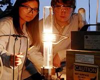
Not long after the development of the first laser in 1960 scientists discovered that shining a beam through certain crystals produced light of a different color; more specifically, it produced light of exactly twice the frequency of the original. The phenomenon was dubbed second harmonic generation. The green laser pointers in use today to illustrate presentations are based on this science, but producing such a beautiful emerald beam is no easy feat. The green light begins as an infrared ray that must be first processed through a crystal, various lenses and other optical elements before it can illuminate that PowerPoint on the screen before you. It was later discovered that applying an electrical field to some crystals produced a similar, though weaker, beam of light. This second discovery, known as EFISH - for electric-field-induced second harmonic light generation - has amounted mostly to an interesting bit of scientific knowledge and little more. EFISH devices are big, demanding high-powered lasers, large crystals and thousands of volts of electricity to produce the effect. As a result, they are impractical for all but a few applications. In a paper published in Science, engineers from Stanford have demonstrated a new device that shrinks EFISH devices by orders of magnitude to the nanoscale. The result is an ultra-compact light source with both optical and electrical functions. Research implications for the device range from a better understanding of fundamental science to improved data communications.
Spring-loaded electrons In most cases, when you shine a light on an atom, the added energy will pull the electron away from the positively charged nucleus very predictably, in a linear fashion, so that when the light is turned off and the electron springs back to its original orbit, the energy released is the same as the light that displaced it. The key phrase here being: "in most cases." When the light source is a high-intensity laser shining on a solid, researchers discovered that the farther the electrons are pulled away from the nuclei the less linearly the light interacts with the atoms. "In other words, the light-matter interaction becomes nonlinear," said Alok Vasudev, a graduate student and co-author of the paper. "The light you get out is different from the light you put in. Shine a strong near-infrared laser on the crystal and green light exactly twice the frequency emerges."
Engineering possibilities For many photonic applications, including signal and information processing, it is desirable to electrically manipulate nonlinear light generation. The new device resembles a nanoscale bowtie with two halves of symmetrical gold leaf approaching, but not quite touching, in the center. This thin slit between the two halves is filled with a nonlinear material. The narrowness is critical. It is just 100 nanometers across. "EFISH requires a huge electrical field. From basic physics we know that the strength of an electric field scales linearly with the applied voltage and inversely with the distance between the electrodes - smaller distance, stronger field and vice versa," said Brongersma. "So, if you have two electrodes placed extremely close together, as we do in our experiment, it doesn't take many volts to produce a giant electrical field. In fact, it takes just a single volt." "It is this fundamental science that allows us to shrink the device by orders of magnitude from the human scale to the nanoscale," said Cai.
Enter plasmonics Engineers have learned to control the direction of the ripples by patterning the surface of the metal in such a way that almost all of the energy waves are funneled inward toward the slit between the two metallic electrodes. The light pours into the crevice as if over the edge of a waterfall and there it intensifies, producing light some 80 times stronger than the already intense laser levels from which it came. The researchers next apply a modest voltage to the metal resulting in the tremendous electrical field necessary to produce an EFISH beam.
Practical applications "Those ones and zeroes are just a switch; one is on, zero is off," said Cai. "As more energy-efficient optical information transport is rapidly gaining in importance, it is not a great leap to see why devices that can convert electrical to optical signals and back are of great value." For the time being, however, the researchers caution that practical applications remain down the road, but they have created something new. "It's a great piece of basic science," said Brongersma. "It is work that combines several disciplines - nonlinear optics, electronics, plasmonics, and nanoscale engineering - into a really interesting device that could keep us busy for awhile." Related Links Stanford School of Engineering Nano Technology News From SpaceMart.com Computer Chip Architecture, Technology and Manufacture
|
. |
|
| The content herein, unless otherwise known to be public domain, are Copyright 1995-2011 - Space Media Network. AFP and UPI Wire Stories are copyright Agence France-Presse and United Press International. ESA Portal Reports are copyright European Space Agency. All NASA sourced material is public domain. Additional copyrights may apply in whole or part to other bona fide parties. Advertising does not imply endorsement,agreement or approval of any opinions, statements or information provided by Space Media Network on any Web page published or hosted by Space Media Network. Privacy Statement |

 del.icio.us
 Digg
Digg Reddit
 Google